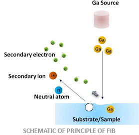
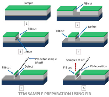
FIB (Focused Ion Beam) is a popular technique in the semiconductor industry and material science for imaging, circuit modification and to prepare precise cross section of sample for STEM and TEM. The FIB instrument is similar to an SEM (Scanning Electron Microscope) but uses a focused ion beam instead of focused electron beam. A finely collimated beam of ions operating at low beam current is generally used for imaging and at higher beam current the FIB can be used for sputtering or milling materials precisely. A dual beam FIB/SEM integrates both ion beam source and electron beam source giving a unique advantage of milling the sample or sputtering material by ion beam and imaging the same at the same time using the electron beam. A progressive FIB milling gives a much clearer idea about the nature of the defect or the failure mode.